32-bit RISC-V CPU from Logic Gates
A complete 2-stage pipelined RV32I processor built from first principles in Logisim: ALU, register file, control unit, and memory system, all hand-wired from basic gates.
A complete 32-bit RISC-V processor built entirely from primitive Logisim gates: no black-box modules, no HDL compiler, every wire placed by hand. Implements the full RV32I base integer ISA across a 2-stage pipeline: Fetch/Decode in stage 1, Execute/Writeback in stage 2.
Datapath
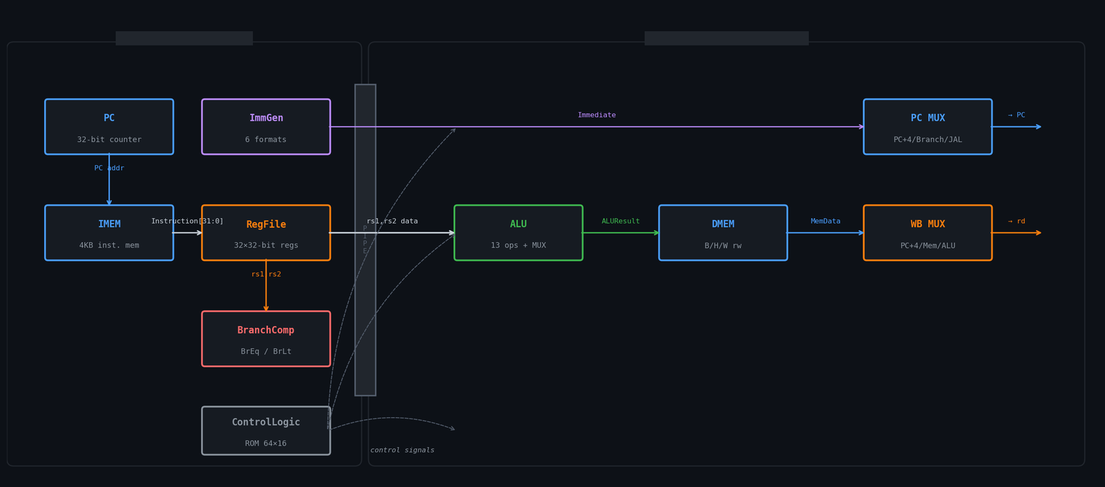
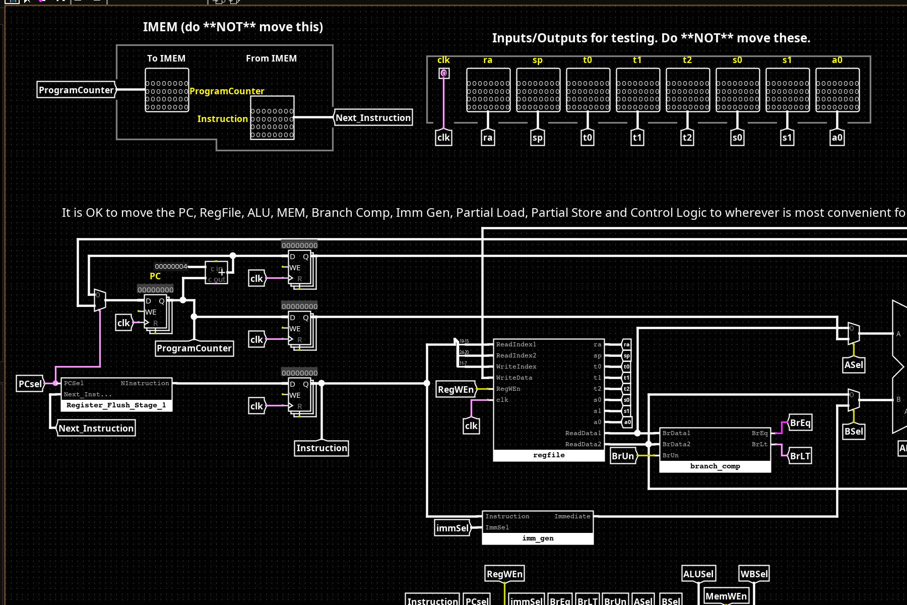
Stage 1 (Fetch/Decode): PC addresses IMEM, returning a 32-bit instruction. The instruction is decoded into register addresses (rs1, rs2, rd), fed to the RegFile for reads, routed through ImmGen to extract the immediate, and analyzed by BranchComp for branch condition evaluation. ControlLogic generates all 10 control signals from the instruction bits.
Stage 2 (Execute/Writeback): The ALU computes using rs1 data and a BSel-muxed second operand (rs2 or immediate). For loads/stores, DMEM is read or written. A WBSel MUX selects the writeback value (ALU result, memory data, or PC+4 for JAL). PCSel selects the next PC (sequential, branch target, or jump target).
Pipeline register: A single register between stages holds the instruction word, PC, and register file outputs. This is where the 2-stage boundary is: Stage 1 is combinational from the PC register; Stage 2 produces the next state.
Instruction Formats
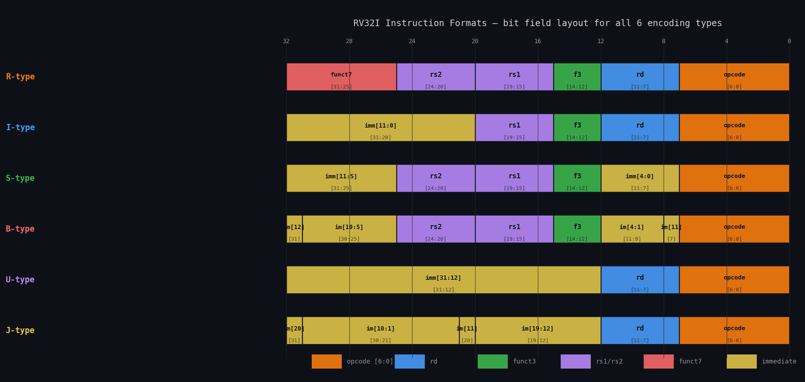
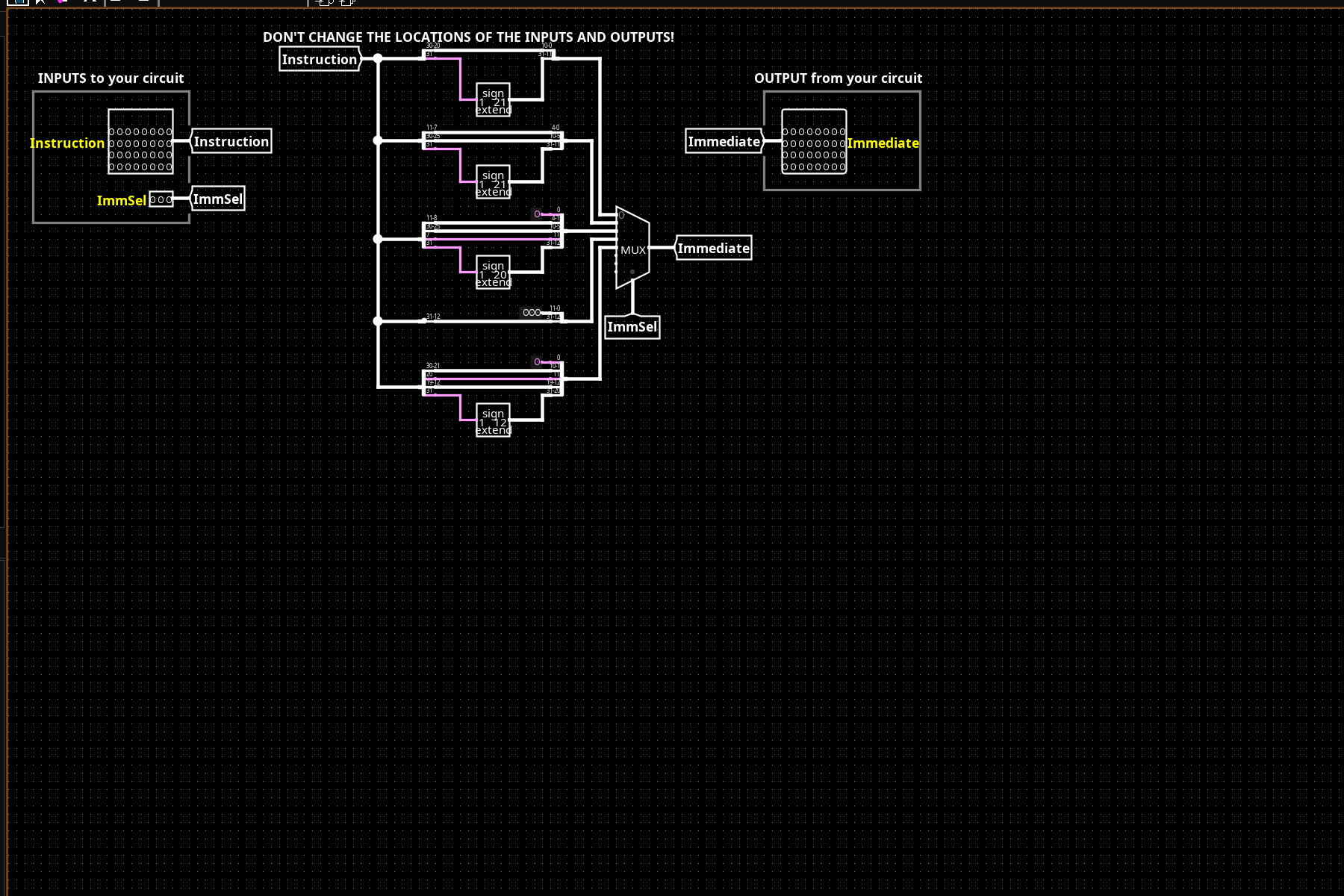
RV32I uses 6 instruction formats, all fixed at 32 bits with a shared opcode field at [6:0]. The immediate fields are deliberately scrambled across formats; bits are arranged so that sign bit [31] is always the MSB of the immediate, minimizing sign extension logic. ImmGen handles the bit-extraction and reassembly for all 6 formats via a 3-bit ImmSel control signal.
ALU
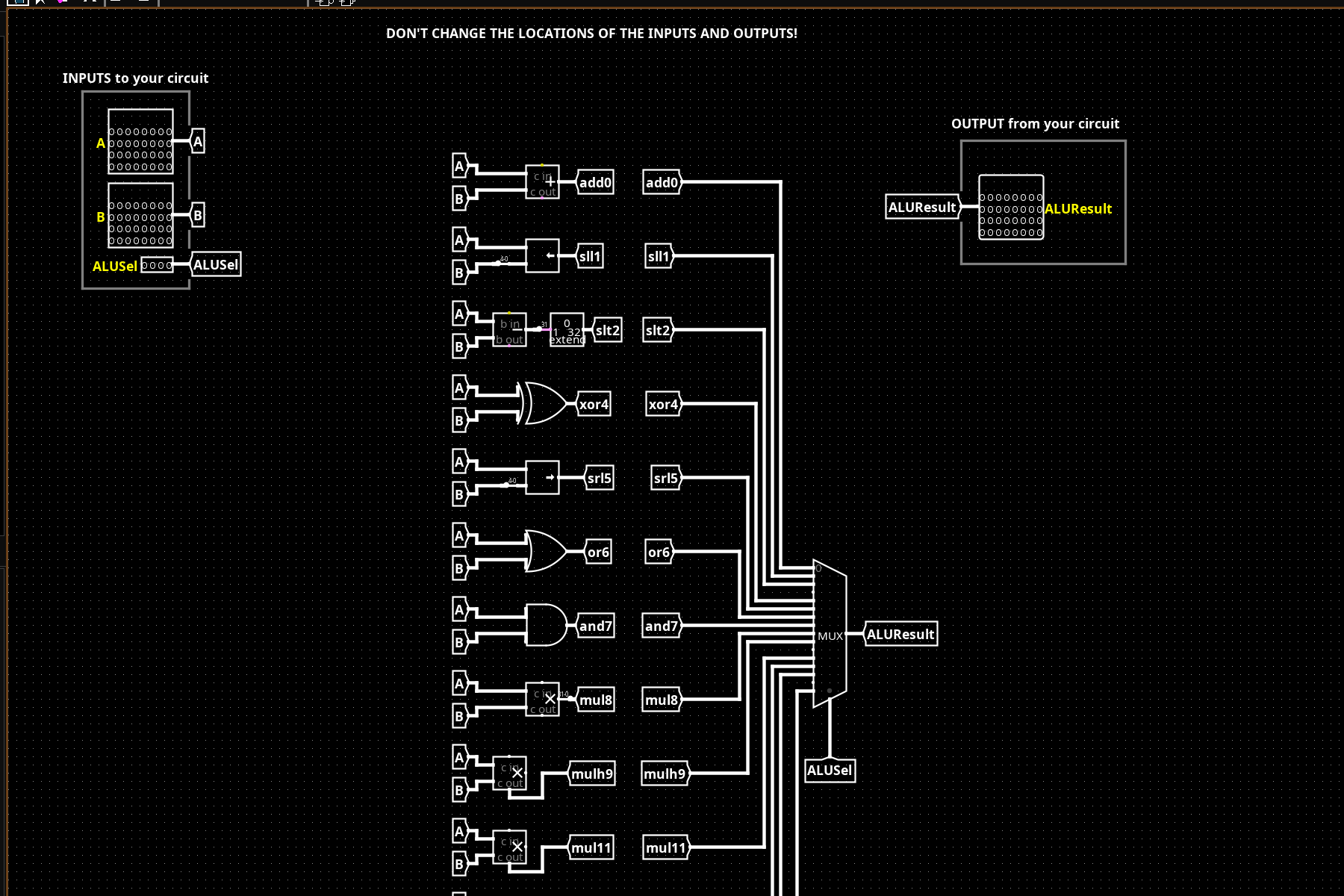
13 operations computed in parallel, selected by a 4-bit ALUSel signal through a final MUX. The ALU implements: ADD, SUB, SLL, SLT, SLTU, XOR, SRL, SRA, OR, AND, MUL, MULH, MULHU. Shift amounts are taken from the lower 5 bits of operand B. Signed comparisons (SLT) use subtraction with overflow-aware interpretation; unsigned (SLTU) use magnitude logic. The parallel-compute-then-select structure keeps the critical path to one operation depth plus MUX.
Register File
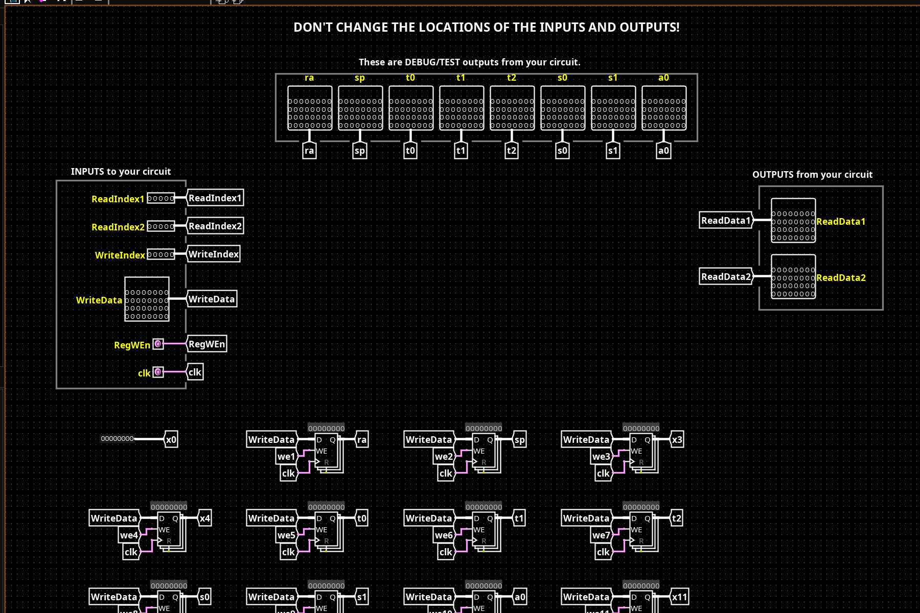
32 × 32-bit registers built from D flip-flop arrays. Two simultaneous read ports (rs1, rs2) via 32-to-1 MUXes; one write port (rd) via a demultiplexer gated by RegWEn and the clock edge. Register x0 is hardwired to zero; writes are silently discarded, reads return 0 unconditionally. The debug output bus at the top exposes ra, sp, t0–t2, s0–s1, and a0 for testing.
Control Logic and Immediate Generator
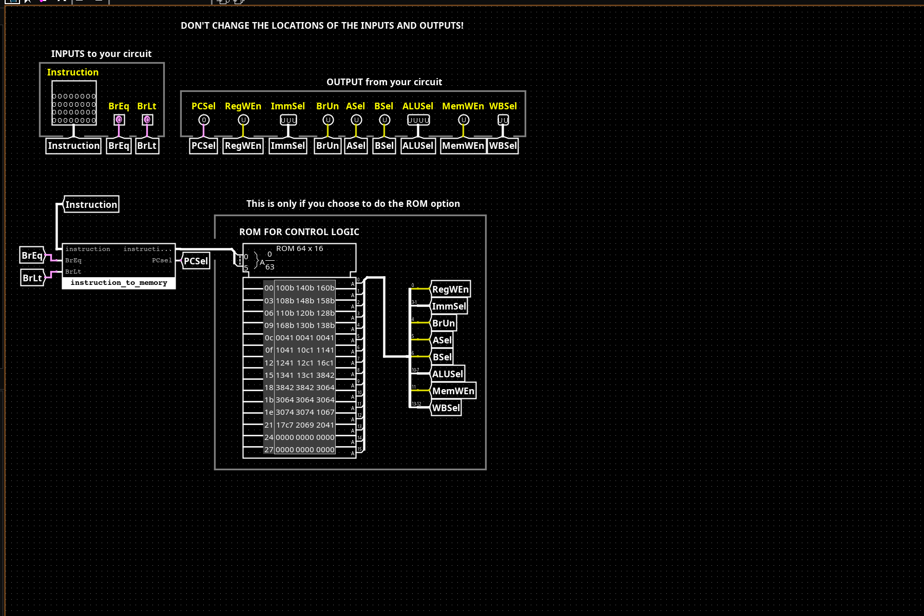
Control (left): A 64×16 ROM addressed by opcode[6:2] + funct3 + funct7[5] produces all 10 control signals in one cycle: PCSel, RegWEn, ImmSel[2:0], BrUn, ASel, BSel, ALUSel[3:0], MemWEn, WBSel[1:0]. ROM-based control is simpler to modify than gate-level decoder trees and keeps the control path short.
ImmGen (right): Extracts immediate bits from the instruction word and sign-extends to 32 bits. Each of the 5 ImmSel cases (I/S/B/U/J) routes different bit slices through sign-extend blocks, then muxes to the output. B-type and J-type require bit reordering (e.g., bit 7 → imm[11], bit 31 → imm[12]) which is why ImmGen is more than a simple extraction.
Branch Comparator
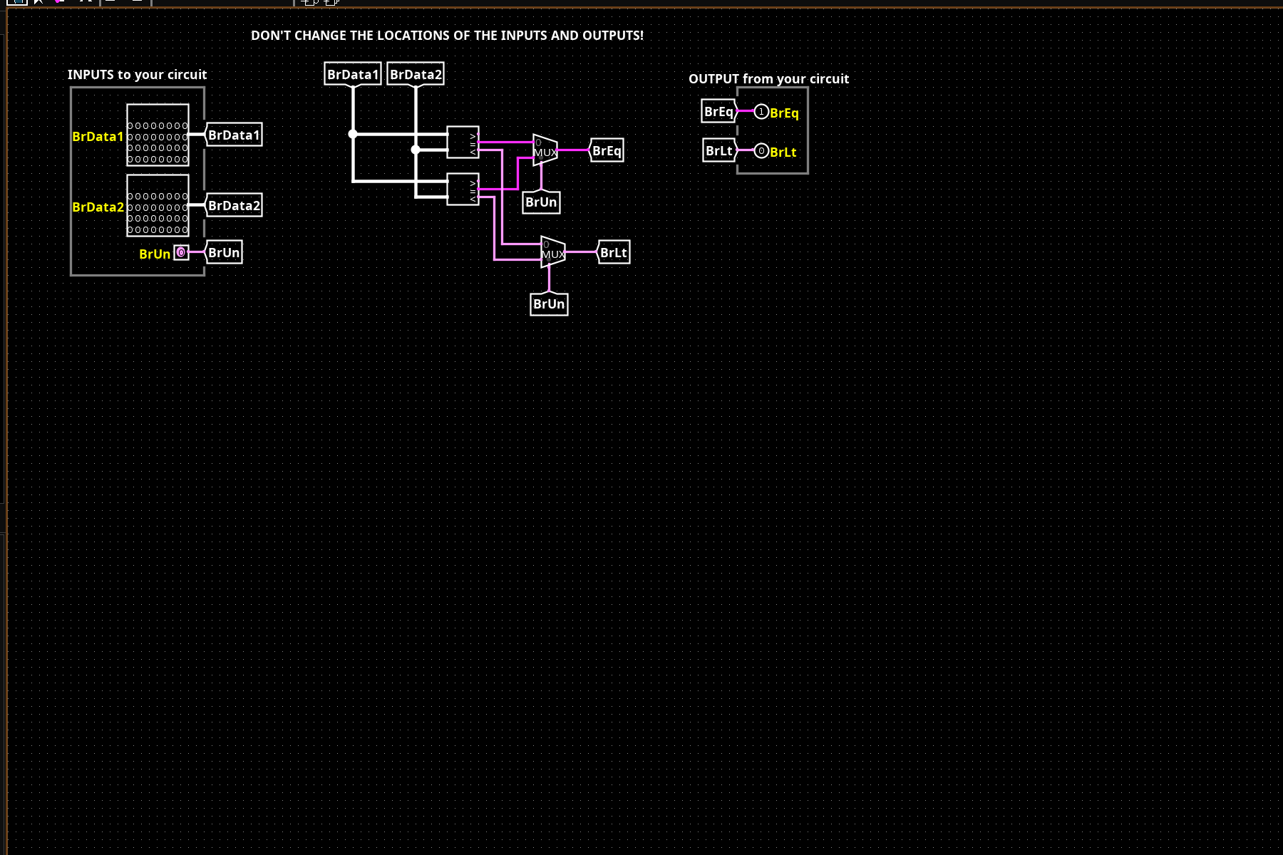
BranchComp evaluates equality and less-than before the ALU, operating on the raw register file outputs. It produces two 1-bit signals: BrEq (BrData1 == BrData2) and BrLt (BrData1 < BrData2). The BrUn control signal switches between signed and unsigned comparisons: unsigned uses magnitude, signed interprets the MSB as a sign bit and adjusts. ControlLogic uses these signals alongside the instruction’s funct3 to assert PCSel for taken branches.
Pipeline Hazards
The 2-stage design eliminates most hazards by construction:
- Structural hazards: Harvard architecture. IMEM and DMEM are separate, so fetch and memory access never conflict.
- Data hazards: Nearly eliminated because most instructions complete writeback before the next instruction reads. Load-use is the only case requiring a stall (one bubble inserted).
- Control hazards: Branch condition is resolved in Stage 1 (BranchComp runs in the fetch/decode stage), so the branch target is known before Stage 2 executes, with no branch misprediction penalty.
The main cost of a 2-stage design vs deeper pipelines: CPI ceiling is 2.0 for non-stalled execution. A 5-stage design achieves lower CPI but requires a full hazard detection and forwarding unit, which is significantly more logic.